Blog
INSIDE INDIA’S CHIP POWERHOUSE: SRMS ENGINEERING STUDENTS EXPLORE THE FUTURE OF SEMICONDUCTORS at SCL CHANDIGARH!
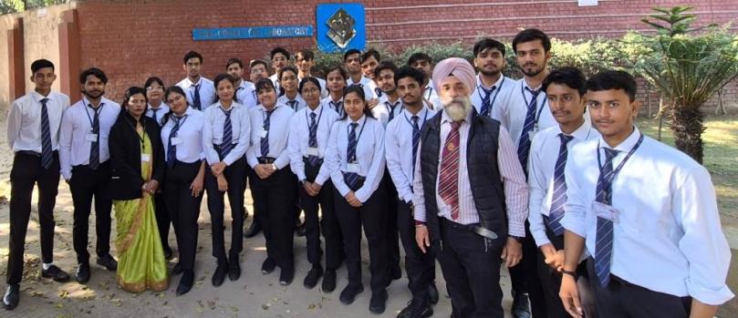
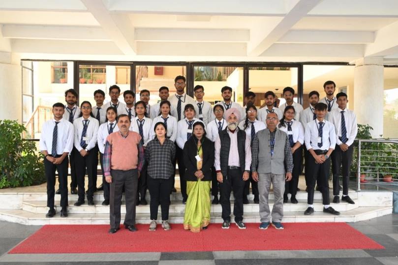
The Department of Electronics & Communication Engineering at SRMS College of Engineering & Technology (CET), Bareilly took a big step into the world of cutting-edge chip technology with an industrial visit to the Semiconductor Laboratory (SCL), Chandigarh, India’s premier Integrated Device Manufacturing Facility under MeitY, Govt. of India.
Organized by the Institution’s Innovation Council (IIC), TDP Cell, and the ECE Department, the visit gave 25 students from 2nd & 3rd year (ECE Department) first-hand exposure to how India is building its semiconductor future. From wafer fabrication to photolithography, packaging, and testing, students explored every stage of chip manufacturing. The SCL scientists also shared insights on India’s proud achievements, including the development of VIKRAM3201 and KALPANA3201, the 32-bit microprocessors created with ISRO for space missions.
However, the team began the journey on 18 November, stayed at Zirakpur, and spent an insightful day inside SCL on 19 November, wrapping the visit with a stop at the scenic Sukhna Lake before returning to Bareilly. A heartfelt thank you to Shri Kulbhusan, HR Head, SCL, for making this visit possible. Experiences like these ignite curiosity, fuel innovation, and inspire young engineers to lead India’s semiconductor mission.